

Blog detail
How to detect defects in ceramic substrates
Release time:
2022-07-18 23:27
How to test the shortcomings of ceramic substrates? China Powder Network News: In the entire process of electronic packaging, ceramic substrates are important components, and reducing the failure rate of ceramic substrates is of great practical significance for improving the quality of electronic components. However, there is no Chinese or national standard for performance testing of ceramic substrates, which poses certain difficulties for the company's production, processing, and brand promotion.
At present, key performance indicators include substrate appearance, structural mechanical properties, thermodynamic properties, electrical properties, encapsulation performance (in operation performance), and stability.
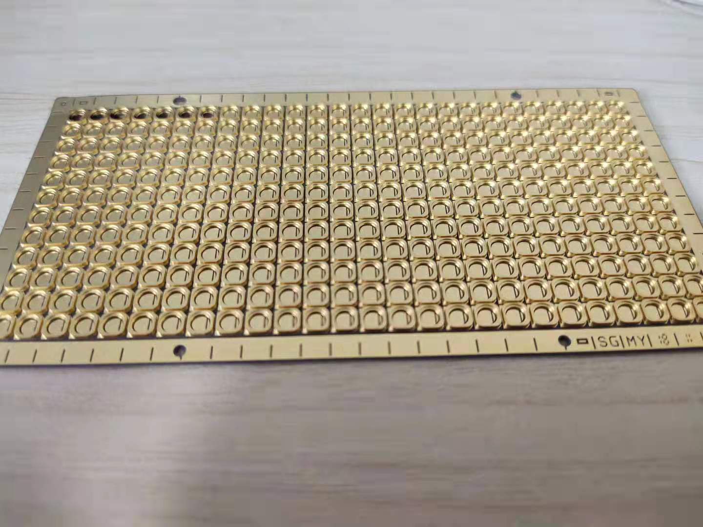
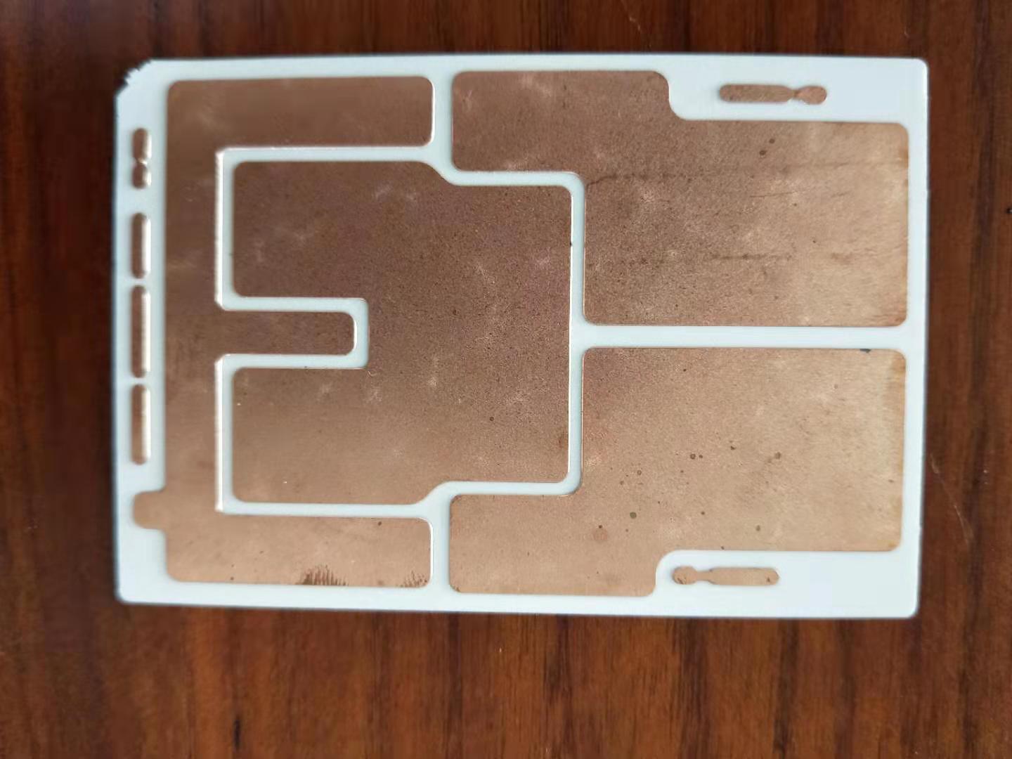
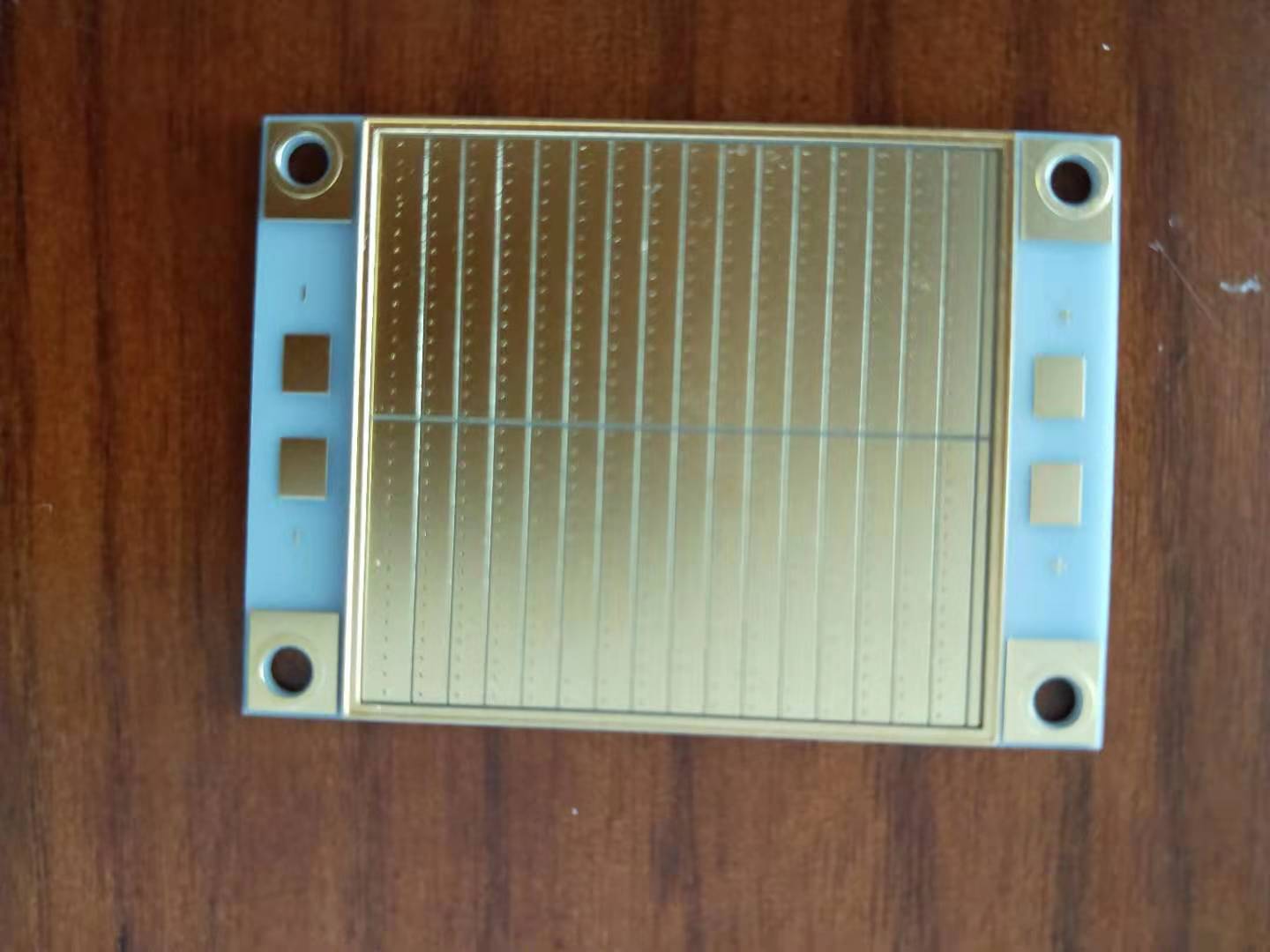
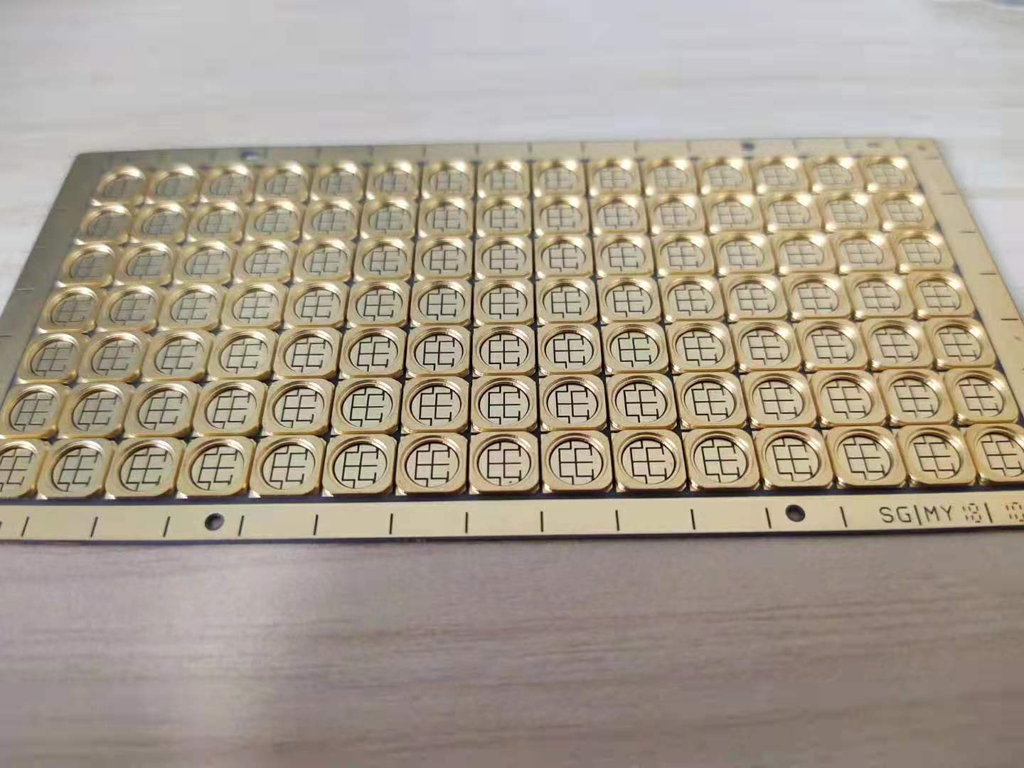
(Image source: 43rd Institute of China Electronics Technology Group Corporation)
Appearance inspection
Appearance inspection generally uses a visual or tool microscope to check whether there are gaps or holes on the surface of the ceramic substrate, and whether there are quality defects such as scratches, peeling, stains, etc. on the surface of the metal layer. In addition, the size and thickness of the ceramic substrate, the thickness of the metal layer, the flatness (expansion and contraction) of the substrate surface, and the precision of the substrate surface pattern are all critical inspection contents. Especially for the selection of inverted sentence integrated ICs and high-density packaging, it is generally required that the surface flatness be less than 3% and the pattern precision be better than 30 μ m.
In recent years, with the continuous development trend of electronic information technology and image recognition technology, the labor cost of the company has continued to soar. In the transformation and development of the processing and manufacturing industry, the company has increasingly attached great importance to the application of artificial intelligence technology and vision systems. According to the inspection methods of machine vision technology and machine equipment, it has gradually become the main way to improve product quality and enhance product qualification rate. Therefore, applying the equipment vision inspection system to the inspection of ceramic substrates can improve inspection precision, reduce labor costs, and have excellent practical value.
Structural mechanical performance testing
The key mechanical properties of the planar ceramic substrate structure refer to the compressive strength of the metal layer fusion, indicating the bonding compressive strength between the metal layer and the ceramic substrate, which immediately affects the post packaging quality of the device (such as solid crystal compressive strength and stability). The fusion compressive strength of ceramic substrates prepared in different ways varies greatly. Generally, flat ceramic substrates (such as TPC, DBC, etc.) made by high-temperature processing technology have higher fusion compressive strength due to the ionic bond connection between the metal layer and the ceramic substrate; The ceramic substrate (such as DPC substrate) produced by ultra-low temperature processing technology is mainly dominated by van der Waals force and mechanical equipment bite force between the metal layer and the ceramic substrate, with slightly lower fusion compressive strength. Common fusion compressive strength testing standards include:
Shear Strength Testing Plan/Tensile Strength Testing Plan
(1) Adhesive tape method: Place the adhesive tape tightly against the surface of the metal layer, and use an eraser roller to press and shape it on top to remove the bubbles on the bonded parallel surface. After 10 seconds, use the tensile strength of vertically dividing the metal layer to detach the adhesive tape, and check whether the metal layer has detached from the silicon wafer, which belongs to a judgment test standard.
(2) Welding wire method: Using metal wires with an outer diameter of 0.5mm or 1.0mm, spot weld them immediately onto the base metal layer according to the melting of the welding material, and then accurately measure the tensile strength of the metal wire in the vertical direction using a tensile strength gauge.
(3) Tensile strength method: Etch (cut) the metal layer on the surface of the ceramic substrate into a 5mm -10mm strip shape, and then tear it off vertically in a tensile strength testing machine to test its tensile strength. The specified detachment rate is 50mm/min, and the precise measurement frequency is 10 times/s.
Thermodynamic performance
The key thermodynamic properties of ceramic substrates include thermal conductivity, temperature resistance, linear expansion coefficient, and heat transfer coefficient. Ceramic substrates are mainly used for heat dissipation in device packaging, so their thermal conductivity is a crucial performance indicator; The key to temperature resistance testing is whether the ceramic substrate undergoes expansion, contraction, or deformation under continuous high temperature, whether the surface metal routing layer undergoes air oxidation, discoloration, blistering, or delamination, and whether the internal buried holes are ineffective. Because ceramic substrates are generally double-layer structures, their heat transfer characteristics are not only related to the thermal conductivity of the ceramic substrate raw materials (bulk heat transfer coefficient), but also closely related to the fusion status of the raw material pages (page touch heat transfer coefficient). Therefore, selecting a heat transfer coefficient detector (which can accurately measure the heat transfer coefficient of the double-layer structure and the heat transfer coefficient of the page) can reasonably evaluate the heat transfer performance of ceramic substrates.
Electric Power Performance
The key to the electrical performance of ceramic substrates lies in whether the metal layers on both sides of the substrate are conductive (whether the quality of the internal buried holes is excellent). Due to the small diameter of the buried holes in DPC ceramic substrates, defects such as unfilled holes and air vents may occur during the electroplating process. Generally, X-ray detectors (for quick judgment) and laser testing machines (for quantitative analysis, cost-effective) can be used to evaluate the quality of buried holes in ceramic substrates.
Packaging performance
The key performance indicators for ceramic substrate packaging are malleability and sealing (limited to three-dimensional ceramic substrates). To improve the compressive strength of wire bonding, a layer of excellent welding performance metals such as Au or Ag is generally electroplated or chemically plated on the surface of the ceramic substrate metal layer (especially the solder layer) to avoid air oxidation and enhance the quality of wire bonding. The malleability is generally measured accurately using aluminum coin automatic welding machines and tensile gauges.
The integrated IC is mounted on a three-dimensional ceramic substrate cavity body, and the internal cavity is sealed with a back cover plate (metal or laminated glass) to complete the device's airtight packaging. The sealing performance of the dam's raw materials and welding materials immediately affects the sealing performance of the device packaging, and there are certain differences in the sealing performance of three-dimensional ceramic substrates prepared in different ways. The key methods for detecting the sealing properties of the dam's raw materials and structural characteristics on three-dimensional ceramic substrates include the fluorine oil bubble method and helium mass spectrometry instrument method.
Reliability testing and analysis
Stability key testing involves the performance transformation of ceramic substrates in specified natural environments (high temperature, ultra-low temperature, high low temperature, radiation source, etching, high-frequency vibration, etc.), including temperature resistance, high temperature storage, high low temperature test cycle system, thermal shock resistance, corrosion resistance, corrosion resistance, high-frequency vibration, etc. For ineffective samples, transmission electron microscopy (SEM) and X-ray diffraction (XRD) can be used to conduct external economic and chemical composition analysis respectively; Use a scanning acoustic optical microscope (SAM) and X-ray inspection instrument to conduct analysis of welding pages and defects.
Reference source:
[1] Cheng Hao, Chen Mingxiang, et al. Ceramic substrates for electronic packaging
[2] Cheng Hao, Chen Mingxiang, et al. Technical and usage progress of ceramic substrates for output power electronic packaging
[3] Huang Sibo. According to HALCON's LED ceramic substrate visual inspection system software
(Compiled by China Powder Network/Qunshan)
Note: The photo is not a commercial activity and there is infringement. Please delete it

Phone: 13528819118
Email: sales@chaoshengpcb-fpc.com
Office address: 101, No.2 Longhe Road,
Longgang District, Shenzhen,
Guangdong, China
(Cha Bajie Headquarters) 2nd Floor
Chaosheng Electronics)
Hong Kong Address: Chungking Mansion,
36-44 Nathan Road, Tsim Sha Tsui, Kowloon,
Hong Kong, China

Sales Department2:616674225
Sales Department销售部:373011007
Tel:+86-13528819118
Email:sales@chaoshengpcb-fpc.com
WhatsApp:13528819118
Skype:pcb-fpcb88@163.com