

Blog detail
Surface treatment process and steps for copper based circuit boards
Release time:
2022-07-19 00:17
Surface treatment process and steps for copper based circuit boards
The surface solution production process and process of copper based circuit boards. Copper substrate surface solution refers to the processing method of artificially creating a layer of surface on the surface of the basic raw material that differs from conventional mechanical equipment, physical and chemical properties.
The purpose of surface treatment is to achieve the corrosion resistance, wear resistance, decoration or other special functional requirements of the product.
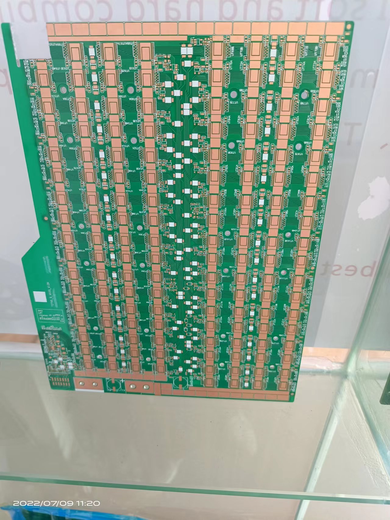
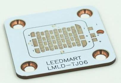
With the rapid development of contemporary automation technology, surface treatment is often used on PCBs. The common PCB surface treatment here refers to the electrical connection and grounding nodes between electronic components or other software on the PCB and the circuit, such as solder layers or touch connections. Bare copper has excellent malleability, but it is highly susceptible to oxidation and environmental pollution when exposed to air. That is also a factor that PCB must carry out surface treatment.
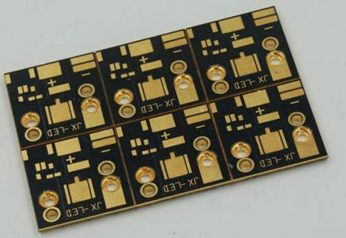
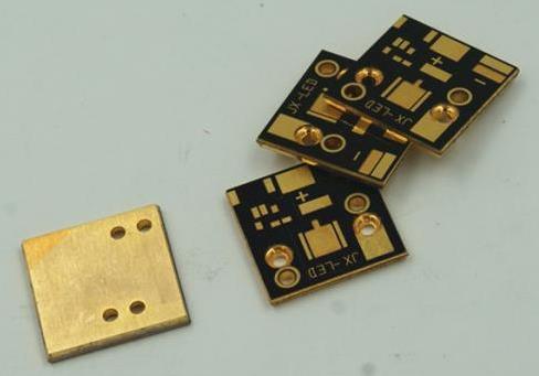
In the production and manufacturing of copper substrates, the processing technology is at a leading level in China. The traditional surface solution production process for copper substrates (taking tin plating as an example) is as follows: issuing materials → grinding plates → sanding cloth → applying high-temperature resistant adhesive → pressing copper paste → drilling holes → shaping the inner groove → primary electroplating process → rinsing → secondary electroplating process → etching process → electrostatic powder spraying → gong appearance design → V-CUT → visual inspection → adhesive peeling → film peeling → outer packaging → tin plating → bending → visual inspection → packaging → warehousing. Because most of the PCB copper coins used require selective gold plating, silver plating, electroplating gold plating, tin plating, and electroplating tin plating on the surface, in order to prevent the bending of the copper coins from not fusing with the adhesive,
To obtain a unique copper substrate with a normal four layer board inside the exposed copper coin at the bending position, it is necessary to apply a layer of high-temperature resistant adhesive on the surface to solve the problem. However, the price of applying high-temperature resistant adhesive is relatively expensive, and it must be manually applied by workers. It is required to be leveled without bubbles. Because it is handmade, there are often problems such as missing or uneven application of adhesive, and uneven wrinkles on the adhesive base, which leads to workers repairing and manufacturing, wasting a lot of labor costs; After tearing off the adhesive, a portion of the colloidal solution remains on the surface of the copper substrate, which poses a great threat to subsequent surface treatments such as tin plating. In addition, the application of high-temperature resistant adhesive consumes a lot of corner residue, and cannot be reused after tearing, wasting a lot of adhesive tape materials.
Technical implementation factors: For the above difficulties, there is a copper substrate surface treatment process that uses high-temperature films that are easy to package, print, dry, and can be easily applied instead of high-temperature adhesives, thereby avoiding the use of expensive high-temperature adhesives and saving raw materials, thereby improving processing technology. The surface treatment of copper substrate includes the following process:
(1) Provide copper substrates that have undergone pre-processing;
(2) Both sides of the copper substrate to be bent are packaged and printed with baking oil and printing ink, and the board is continuously baked at high temperature;
(3) Apply browning solution to brown the surface of copper substrate;
(4) Press and punch the copper substrate covered with baking oil printing ink;
(5) After the appearance of the finished product is produced, a electroplating process is carried out;
(6) Carry out surface route fabrication on copper substrates;
(7) Ink printing on copper substrates;
(8) After the appearance of the second gong finished product, V-CUT production will be carried out;
(9) Surface treatment is carried out at the bending point on the copper substrate;
(10) Obtaining finished products by bending and manufacturing copper substrates;
(11) Carry out external research on finished copper substrates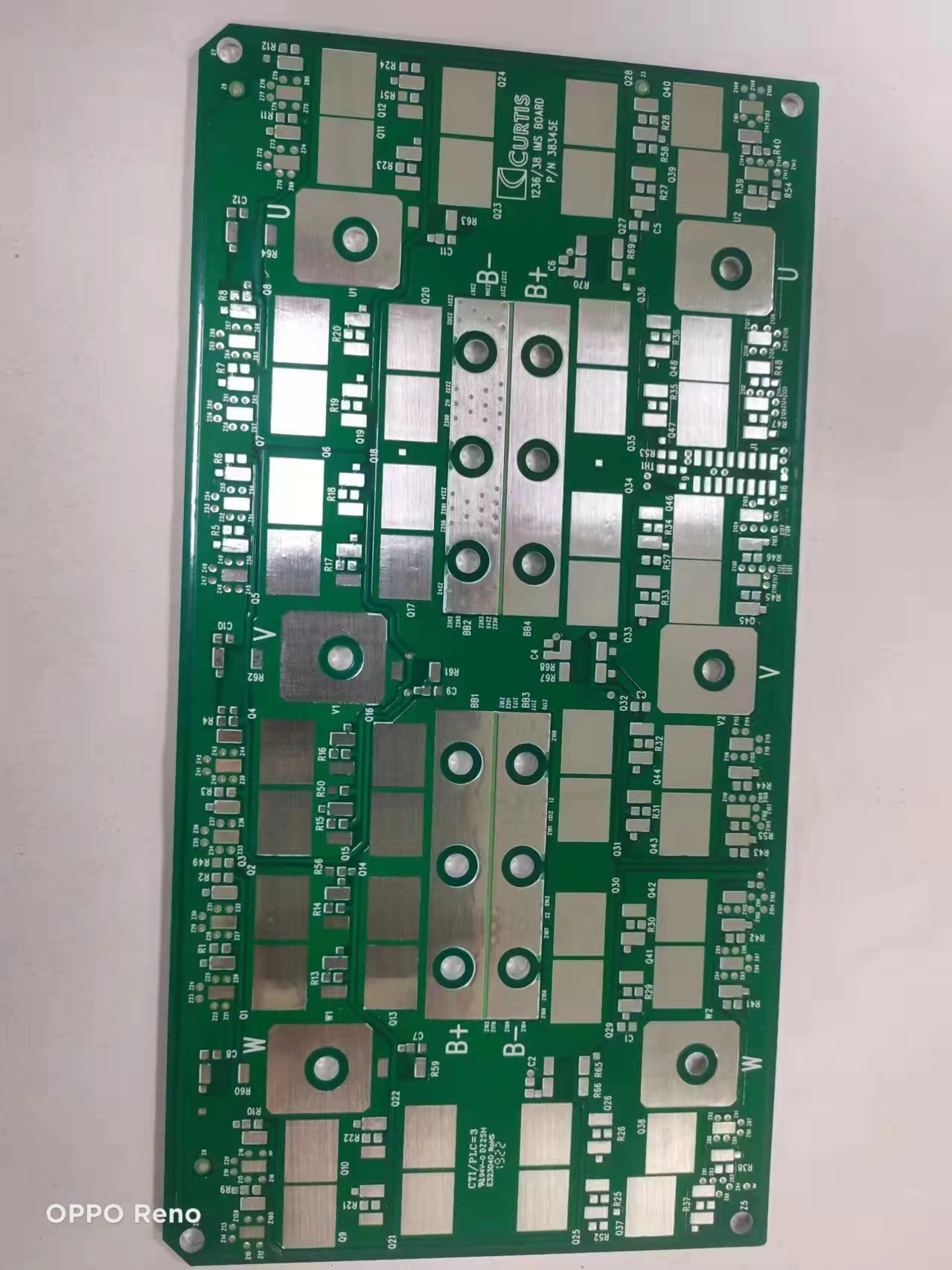


Phone: 13528819118
Email: sales@chaoshengpcb-fpc.com
Office address: 101, No.2 Longhe Road,
Longgang District, Shenzhen,
Guangdong, China
(Cha Bajie Headquarters) 2nd Floor
Chaosheng Electronics)
Hong Kong Address: Chungking Mansion,
36-44 Nathan Road, Tsim Sha Tsui, Kowloon,
Hong Kong, China

Sales Department2:616674225
Sales Department销售部:373011007
Tel:+86-13528819118
Email:sales@chaoshengpcb-fpc.com
WhatsApp:13528819118
Skype:pcb-fpcb88@163.com