

Blog detail
IC Packaging Substrate Technology
Release time:
2022-06-21 11:34
With the miniaturization, multifunctionality, and high-frequency and high-speed digitalization of electronic products, PCB is required to rapidly move towards high-density, high-performance, and high reliability development. In order to meet this requirement, not only have PCBs rapidly moved towards HDIBUM boards, embedded (integrated) component PCBs, etc., but IC packaging substrates have also rapidly moved from inorganic substrates (ceramic substrates) to organic substrates (PCB boards). Organic IC packaging substrates are developed by further deepening (high-density) on the basis of HDI/BUM boards, or IC packaging substrates are HDI/BUM boards with higher density.
IC Packaging Substrate Technology
With the miniaturization, multifunctionality, and high-frequency and high-speed digitalization of electronic products, PCB is required to rapidly move towards high-density, high-performance, and high reliability development. In order to meet this requirement, not only have PCBs rapidly moved towards HDIBUM boards, embedded (integrated) component PCBs, etc., but IC packaging substrates have also rapidly moved from inorganic substrates (ceramic substrates) to organic substrates (PCB boards). Organic IC packaging substrates are developed by further deepening (high-density) on the basis of HDI/BUM boards, or IC packaging substrates are HDI/BUM boards with higher density.
Proposal and types of packaging substrates
1.1 Proposal of Organic Packaging Substrate
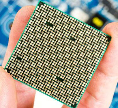
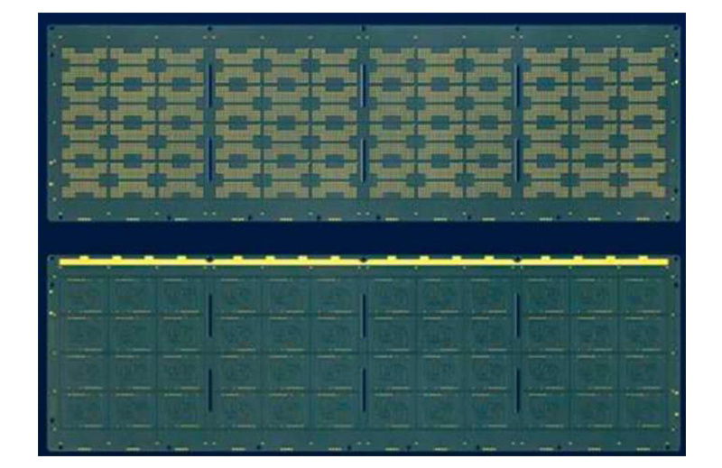
A packaging substrate is a type of substrate used to repackage and assemble multiple primary (or secondary) packaged IC components into a higher density and capacity. Due to the high packaging density of these substrates, their sizes are not large, mostly ≤ 50 * 70mm2. In the past, ceramic substrates were mainly used, but now we are rapidly moving towards high-density PCB packaging substrates.
(1) Ceramic packaging substrate.
The application of ceramic packaging substrates has a history of several decades, with the advantages of small CTE and high thermal conductivity. However, with the development of high-density, especially high-frequency and high-speed digitalization of signal transmission, ceramic packaging substrates have encountered severe challenges.
① The dielectric constant ε r is large (6-8).
The signal transmission speed V is determined by the dielectric constant ε r, as shown in the following equation.
V=k·C/(εr)1/2
Among them: k - is a constant; C - speed of light. This means that using a smaller dielectric constant ε r can result in higher signal transmission speeds. There are also issues such as characteristic impedance values.
② Low density. L/S≥O.1mm, Due to its thick thickness and large aperture, it cannot meet the requirements for high integration of ICs.
③ High resistance. Most wires are made of molybdenum, which has a resistivity (after sintering) that is more than three times or more higher than copper, generates a large amount of heat, and affects electrical performance.
④ The substrate size cannot be large, as it affects the density and capacity improvement. Due to the high brittleness of ceramic substrates, not only can the size not be large,
Moreover, extra caution is required in production, assembly, and application.
⑤ Difficulty in thinning. The thickness is relatively thick, mostly above 1mm.
⑥ High cost.
(2) Organic (PCB) substrate.
Organic (PCB) substrates are exactly opposite to ceramic packaging substrates.
① The dielectric constant ε r is small (with high selectivity, mostly using 3-4 materials).
② High density is good. L/S can reach 20-50 μ m, with a thin dielectric layer and small pore size.
③ Low resistance. Low heat generation and good electrical performance.
④ The substrate size can be expanded. Most of them are ≤ 70 * 100mm2.
⑤ Thinning is possible, currently, double-sided/four layer boards can reach 100-300 μ m.
⑥ Low cost.
In 1991, the PCB and HDI/BUM board developed by the Nozoku Research Institute in Japan for resin sealed inverted chip mounting and inverted chip bonding (connection). These organic packaging substrates and HDI/BUM boards have superior advantages and conditions compared to ceramic substrates, making them very suitable as bare chip packaging substrates for ICs, especially for the packaging of metal wires for inverted chips (FC). They not only solve the CTE matching problem of packaging, but also solve the feasibility problem of high-density chip installation.

Phone: 13528819118
Email: sales@chaoshengpcb-fpc.com
Office address: 101, No.2 Longhe Road,
Longgang District, Shenzhen,
Guangdong, China
(Cha Bajie Headquarters) 2nd Floor
Chaosheng Electronics)
Hong Kong Address: Chungking Mansion,
36-44 Nathan Road, Tsim Sha Tsui, Kowloon,
Hong Kong, China

Sales Department2:616674225
Sales Department销售部:373011007
Tel:+86-13528819118
Email:sales@chaoshengpcb-fpc.com
WhatsApp:13528819118
Skype:pcb-fpcb88@163.com