

Blog detail
Integrated IC Packaging Circuit Board Technology
Release time:
2022-06-21 11:46
IC packaging refers to the process of connecting circuit pins on a silicon wafer to external connectors using wires for connection with other devices. The packaging form refers to the outer shell used for installing semiconductor integrated circuit chips.
Integrated IC Packaging Circuit Board Technology
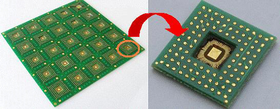
IC packaging refers to the process of connecting circuit pins on a silicon wafer to external connectors using wires for connection with other devices. The packaging form refers to the outer shell used for installing semiconductor integrated circuit chips. It not only plays a role in installing, fixing, sealing, protecting chips, and enhancing thermal performance, but also connects to the pins of the packaging shell through the contacts on the chip with wires. These pins are then connected to other devices through wires on the printed circuit board, thus achieving the connection between the internal chip and the external circuit. Because the chip must be isolated from the outside world to prevent impurities in the air from corroding the chip circuit and causing a decrease in electrical performance.
BGA products were developed in the 1990s. Compared to traditional packaging, BGA architecture has the advantages of good heat dissipation and electrical performance, and can greatly increase the number of pins. BGA packaging has given rise to different product forms, such as CBGA (Ceramic BGA), PBGA (Plastic BGA), TBGA (Tape BGA), etc. PBGA uses resin substrate, which is low in price and has good heat resistance, making it easy to become a carrier board for ICs.
Manufacturing process.
The manufacturing process of IC card packaging framework is a high-precision and complex process. Currently, there are few factories in China that produce it, and the basic materials used in the production process mainly rely on imports. The specific production and processing process is as follows: first, a high-speed precision punch is used to punch out the corresponding vacancies on the glass fiber substrate according to the design requirements, then the conductive materials are bonded together through precision film sticking equipment, and the designed pattern is exposed on its surface using photography technology. Finally, the finished product is formed through corresponding post-processing processes.
SiP (System in Package) is defined similarly to MCM (Multi chip Module). SiP refers to the encapsulation of component systems, which can include chips or RCL passive components, or even other modules. It can also combine different technologies such as PiP (Package in Package), PoP (Package on Package), Stack, etc. Different bonding technologies such as wire bonding, Flip Chip, Hybrid type, etc. have a wide definition. MCM focuses on multi chip co packaging, mainly compared to the previous BGA to Flip Chip BGA style single-chip packaging. In addition, Embedded technology is an important technological development, which can embed active (IC) and passive (mainly RCL passive components) on embedded components. At present, the technology of embedding RCL passive components is relatively mature, and the process can be divided into two categories: bare technology that directly SMD RCL components onto substrates and then film them, and embedded technology that uses no components (replacing RCL with materials). Due to the development of SiP technology for many years, the feasibility of transferring from current packaging technology is high, and it can significantly reduce the size and improve signal reliability. Therefore, it will be widely used in Handset products, and after the establishment of mass production lines, it will quickly spread to other products.


Phone: 13528819118
Email: sales@chaoshengpcb-fpc.com
Office address: 101, No.2 Longhe Road,
Longgang District, Shenzhen,
Guangdong, China
(Cha Bajie Headquarters) 2nd Floor
Chaosheng Electronics)
Hong Kong Address: Chungking Mansion,
36-44 Nathan Road, Tsim Sha Tsui, Kowloon,
Hong Kong, China

Sales Department2:616674225
Sales Department销售部:373011007
Tel:+86-13528819118
Email:sales@chaoshengpcb-fpc.com
WhatsApp:13528819118
Skype:pcb-fpcb88@163.com