

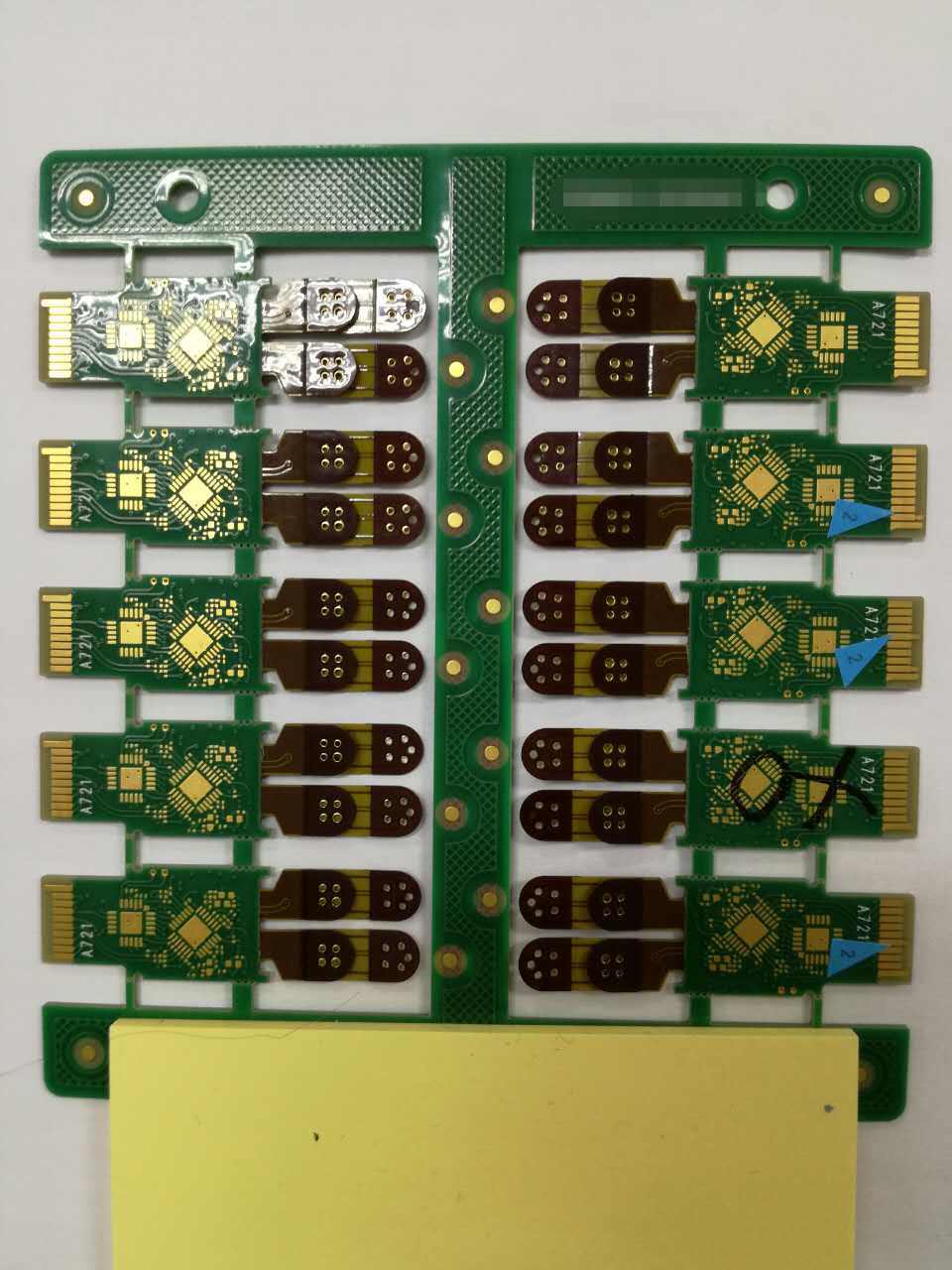
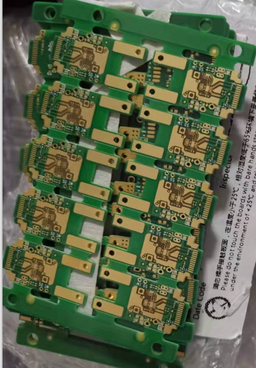
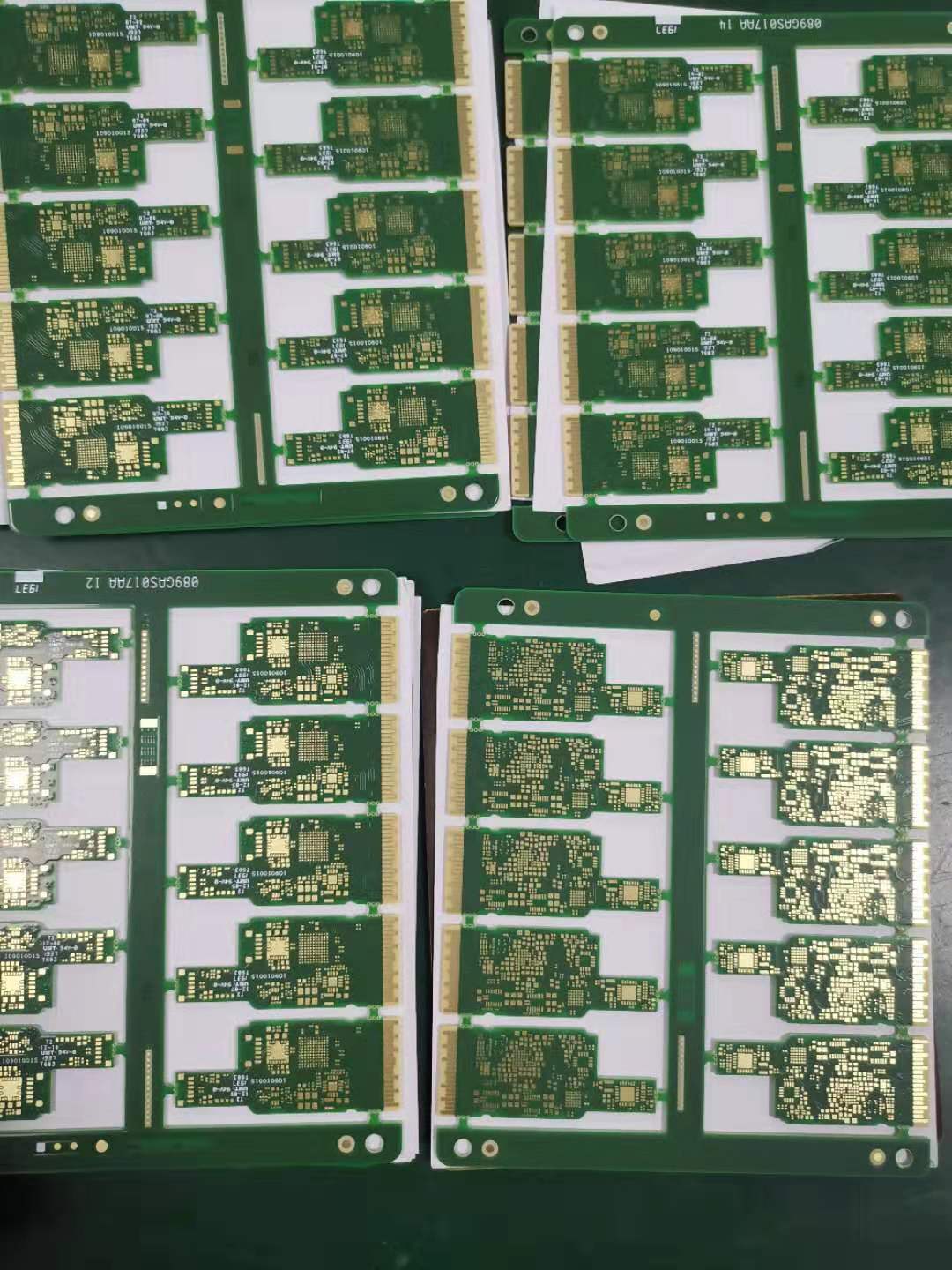
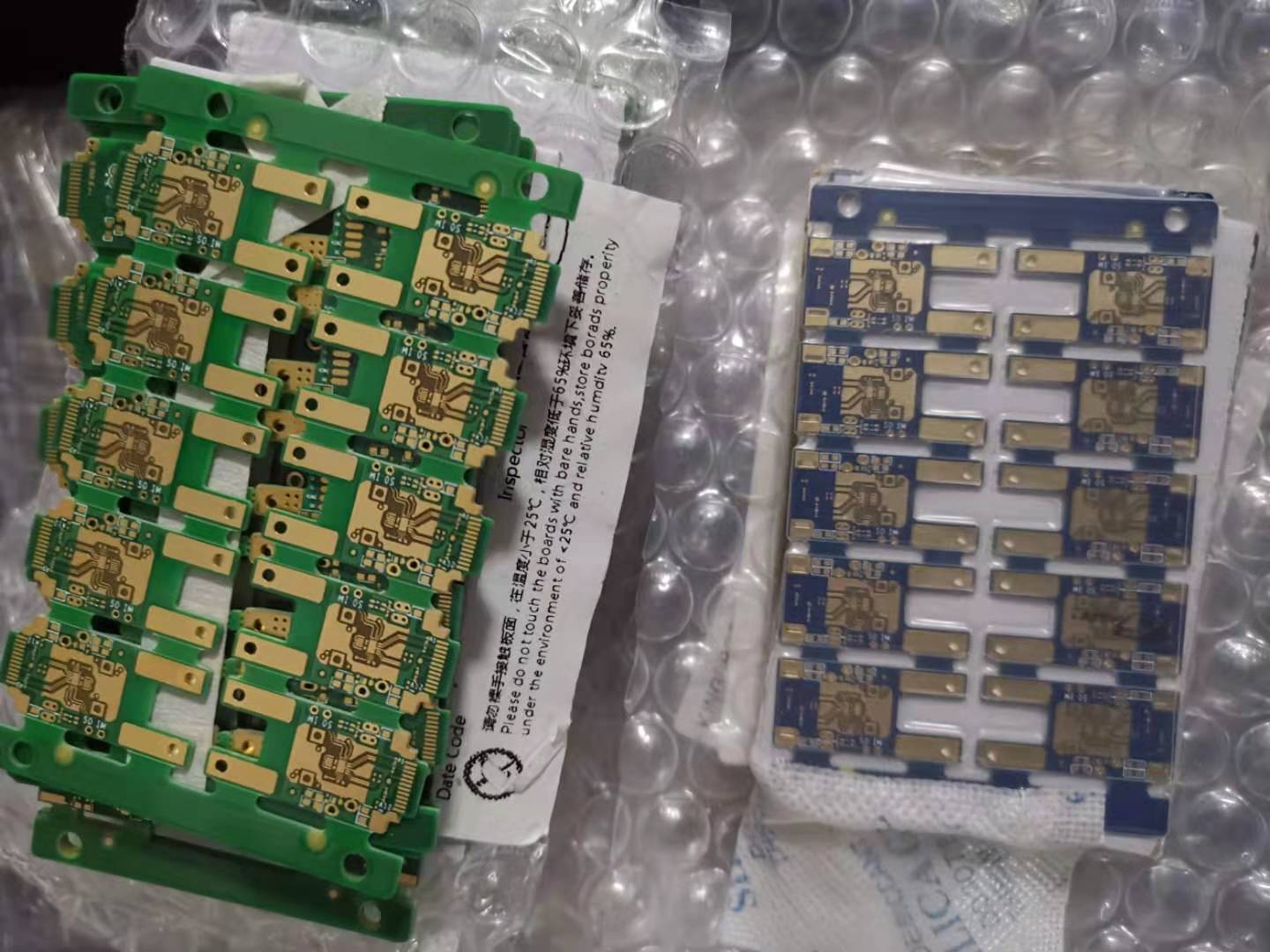
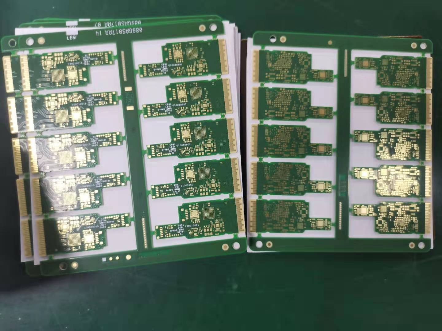
Optical communication, optical module, embedded high-speed,16L oversized military antenna board

key word:

Product consultation:

Product Description

Optical communication, optical module, embedded high-speed,16L oversized military antenna board
Product field: Satellite 2 camera PCB
Layers: 2L oversized military antenna board
Plate thickness: 3.20mm
Size: 1150*1150mm/1*1PCS
Process structure: FR-4, TG135, copper thickness 20um
Minimum hole 0.15mm
Minimum line width line spacing 4/5mil
Surface treatment: Electro-nickel gold 1U"

Main Product Structure of Chaosheng Group Company
Production of 2-80 layer rigid circuit boards, 2-50 layer flexible circuit boards, and PCBA
Main product categories of Chaosheng Group Company
High end double-sided, multi-layer, flexible, high-frequency, HDI arbitrary interconnection, metal substrate, high thermal conductivity metal substrate, ceramic, cut into metal substrate, cut into buried capacitor, cut into thick copper buried magnet, concave convex step substrate, 5G high-speed board, thick copper, thick gold, high carbon resistance, double-sided multi-layer MiNiLED, MiNiHDILED, MiNiOLED, IC carrier substrate, roll on roll FPC, long FPC, large-sized printed circuit board, halogen-free materials, high-frequency materials, high-speed materials Metal materials, environmentally friendly circuit boards, blind buried through-hole circuit boards, high thermal conductivity aluminum based, thermoelectric separation copper based, PDU bus, iron-based and metal based (core) hybrid boards, embedded copper buried, buried resistance and capacitance ceramic bead boards, ultra-thin BT boards, ceramic substrates, IC carrier boards, high-frequency hybrid voltage, high-speed boards, differential resistance boards, thick copper plates, thick gold-plated plates, HDI, Anylayer in any order (cross blind buried), double-sided, multi-layer, HDIFPC, soft and hard HDI, Integrated OEM and ODM production factories for roll to roll FPC, ultra long FPC, ultra large PCB production and product design and development, software development, and special material printed circuit boards.
The main application areas of PCB and PCBA products of Chaosheng Group Company
Communication terminals, communication stations, electronic communication, fiber optics, optical modules, backlights, chip systems, communication equipment, communication instruments, computers, intelligent devices, intelligent control, system control, industrial power control, industrial equipment, testing instruments, testing instruments, SD cards, SG cards, mobile phones, computers, various antennas, radars, automobiles, light sources, mold proof, music equipment, playback equipment, banking equipment, medical equipment Medical devices, medical equipment, aerospace, aviation, military, LED, OLED, OLCD power control power supply, industrial power supply, communication power supply, automotive power supply, office equipment, digital products, computers and other application fields;
The main application areas of flexible circuit boards (FPC) and FPCA products of Chaosheng Group
CompanyHard disk drives, printers, fax machines, scanners, sensors, mobile phones, connectors, modules, walkie talkie antenna cards, high-end cameras, digital cameras, laser heads, CDs, medical, instrument, driver, automotive, automotive instruments, automotive hard drives, drivers, CD drivers, medical equipment, medical equipment, LED light strips, military, aviation, aerospace, national defense and other product fields.
NO    project    Process Capability
1    Layers    1-80Layers
2    Maximum size of PCB    2500*1150mm
3    Maximum size of flexible FPC    500mm*100Meter
4    Maximum size of PCBA    1600mm*1000mm
5    Maximum size of FPCBA    500mm*100Meter
6    PCB Finished Thickness    0.15-12.0mm
7    Flexible FPC Finished Thickness    0.05-0.60mm
8    Finished sheet copper thickness    12um-1075um
9    Laser hole minimum diameter    0.075mm
10    Minimum line width and line spacing    1.5mi/1.50mil
11    Through hole minimum finished diameter    0.15mm
12    Thickness Stack Aspect Ratio    1:35
13    by processing method    VIA hole blind buried hole treatment: ink plug hole, resin plug hole, copper paste plug hole, VCP copper fill hole, silver paste plug hole, carbon oil plug hole, etc.
14    surface treatment     Immersion gold, electro-nickel gold, electro-thick gold, immersion gold + OSP, electro-nickel-gold + immersion gold, electro-nickel-gold + immersion gold + OSP, electro-gold + OSP, immersion gold + gold finger, OSP + gold finger, lead-free spray Tin, lead-free spray tin + immersion gold, lead-free spray tin + gold finger, lead spray tin, OSP, immersion tin, immersion silver, electric silver
15    Main Substrate Brands    Rogers, Arlon, Taconic, TP-2, Megtron, Neclo, Isola, F4B, 3M, Mitsui Group, Taiyao, Taiguang, Tenghui, Shengyi, Lianmao ITEQ, NOUYA, DuPont, Taihong, Hongren, Xin Yang , Nippon Stee, Teflon, Yasen, Matsushita, RCC, 3M Location, CERADIR, Jiuhe, Jiuhao, Zhongci, Huaqing, Ai Shengda, Slitton, Kai Changde, Tongxin, Bergs, Caird, Yalong, Taicani, etc.
16    Solder mask color    Green, Black, Red, Yellow, White, Blue, Purple, Matte Green, Matte Black, Clear, etc.
17    test service    AOI, X-Ray, withstand voltage test, short pass test, solder test, thermal shock test, functional test, high temperature and humidity test, first article tester, etc.
18    Forming method    CNC shape, die punch shape, V-CUT+ molding method
19    Finished warpage    ≤0.5%
20    Mechanical Bore Tolerance    ≤0.025mm
21    Finished warpage    ≤0.5%
22    MiNiLED Minimum PAD    0.065mm/0.065mm
23    Thermal Conductivity    ≧8W
24    The highest pressure    2500Pa
25    High carbon resistance value and tolerance    ≧100→15000Ω±20%
26    Impedance tolerance    ≤5→8%Ω
27    IC carrier substrate series    IC carrier substrate series
                                                                            
FAQ
Question point    answer
Q: What information does the PCB need to provide?    CEGSATE: It is necessary to provide the Gberber file for making PCB, the product process production instructions, such as material requirements, surface treatment requirements, finished product thickness requirements, PCB stack structure diagrams for high-end products, copper thickness requirements for each layer, sample quantity requirements, and bulk order requirements , product application fields and other related information
Q: What information does PCBA need to provide?    CEGSATE: It is necessary to provide BOM report (requires the brand, specification and model of the component), X, Y coordinate number of PCBA components, and processing requirements: Do you need us to purchase components? Or customer-supplied components? Is software burning required? How much is required? Details such as what is the monthly demand.
Q: Are my documents safe?    CEGSATE: Your documents are very secure and we protect intellectual property for our clients throughout the process. All files provided by customers will never be shared with any third party.
Q: How much is the PO MOQ?    CESGATE: There is no MOQ in POE. We have the flexibility to handle both small and large batches.
Q: Do you have other services?    CESGATE: We mainly focus on the procurement services of PCB+FPC production+SMT+Assembly PCBA+components; in addition, we can also provide programming, testing, software programming, wiring, shell assembly services; as well as product design, product development, software development
Q: What is your inspection method? How do you control the quality?    CESGATE: In order to ensure the quality of PCB and FPC products, samples and small batches are usually detected by flying probe; the inner layer circuit passes AOI optical inspection, online AOI inspection, the finished product is 100% tested by E-SET test frame, and the appearance is fully automatic Finished product inspection equipment 100% full inspection and FQC 100% full inspection, PCBA automatic optical inspection (AOI), BGA parts X-Ray 100% ray inspection, first article inspection (FAI), PCBA products that require programming software, according to product functional requirements, 100% full test through the finished test frame, etc.

Related products

China Chao Sheng Electronic Automotive-Grade Hard-Soft Combined HDI-FPC


Automotive electronics PCB, Medical equipment circuit board, Industrial control PCB, Aerospace & military grade PCB, Ion‑equipment high‑voltage board, High‑speed server PCB, 5G communication circuit board, Radar RF microwave PCB, Wireless terminal motherboard, Industrial SBC mainboard, High‑power industrial control PCB, Automation controller board, Drone flight‑control PCB, Robot control board, High frequency low loss PCB, Thick hard gold finger circuit board

China Chaosheng Electronic Intelligent Products Multilayer Circuit Board HDIPCB TechnologyPCB


Automotive electronics PCB, Medical equipment circuit board, Industrial control PCB, Aerospace & military grade PCB, Ion‑equipment high‑voltage board, High‑speed server PCB, 5G communication circuit board, Radar RF microwave PCB, Wireless terminal motherboard, Industrial SBC mainboard, High‑power industrial control PCB, Automation controller board, Drone flight‑control PCB, Robot control board, High frequency low loss PCB, Thick hard gold finger circuit board, HDI blind & buried via PCB

China Chaosheng Electronic and Electrical Products Multi layer Circuit Board PCB Source FactoryPCB


Automotive electronics PCB, Medical equipment circuit board, Industrial control PCB, Aerospace & military grade PCB, Ion‑equipment high‑voltage board, High‑speed server PCB, 5G communication circuit board, Radar RF microwave PCB, Wireless terminal motherboard, Industrial SBC mainboard, High‑power industrial control PCB, Automation controller board, Drone flight‑control PCB, Robot control board, High frequency low loss PCB, Thick hard gold finger circuit board, HDI blind & buried via PCB

China Chaosheng Electronic Medical Equipment Products Multilayer Circuit Board HDIPCB Technology


Automotive electronics PCB, Medical equipment circuit board, Industrial control PCB, Aerospace & military grade PCB, Ion‑equipment high‑voltage board, High‑speed server PCB, 5G communication circuit board, Radar RF microwave PCB, Wireless terminal motherboard, Industrial SBC mainboard, High‑power industrial control PCB, Automation controller board, Drone flight‑control PCB, Robot control board, High frequency low loss PCB, Thick hard gold finger circuit board, HDI blind & buried via PCB

China Chaosheng Electronic Automotive Products Multi layer Circuit Board HDIPCB Technology


Ultra thin PCB,Double layer ultra-thin PCB,Multi layer ultra-thin PCB,HDI ultra-thin PCB,Oversized thin board PCB,Flexible Rigid PCB,PCB factory,Top PCB Manufacturers,Printed Circuit Board (PCB),If you get rid of the PCB,PCB Piezotronics,PCB Simulation,Certified PCB Design Company,Quick Turn PCB

China Chaosheng Automotive Control Multi layer Circuit Board PCB Source Factory


Ultra thin PCB,Double layer ultra-thin PCB,Multi layer ultra-thin PCB,HDI ultra-thin PCB,Oversized thin board PCB,Flexible Rigid PCB,PCB factory,Top PCB Manufacturers,Printed Circuit Board (PCB),If you get rid of the PCB,PCB Piezotronics,PCB Simulation,Certified PCB Design Company,Quick Turn PCB

China Chaosheng Electronics Mobile Phone Flexible Motherboard FPC


any order HDI soft hard combined FPC, blind buried hole HDIFPC, single-layer flexible FPC, double-layer flexible FPC, multi-layer flexible FPC, multi-layer flexible HDIFPC, soft hard combined flexible FPC, soft hard combined HDI flexible FPC, any order HDI soft hard combined flexible FPC

China Chaosheng Electronic Printer Driver Flexible FPC


Ultra long flexible FPC,Ultra long double-layer flexible FPC,Ultra long multi-layer flexible FPC,Ultra long combination of soft and hard FPC,Multi layer ultra long flexible FPC,Ultra long flexible multi-layer FPC,Ultra large flexible FPC,Ultra large flexible multi-layer FPC,Roll to roll flexible FPC, single-layer roll to roll flexible FPC, double-layer roll to roll flexible FPC

China Chaosheng Electronics | Ultra Large&Ultra Long Sizes · Roll to Roll (R-to-R) Flexible FPC Complete Technical Description


Roll‑to‑Roll(R2R) FPC, Ultra‑long flexible circuit board, Max length 15meter FPC, Large format flex PCB, Seamless one‑piece long flex cable, Dupont PI FPC, Thick hard‑gold finger FPC, Multi‑layer long flex PCB, Automotive BMS flexible ribbon, Industrial automation long‑distance flex interconnect

China Chaosheng Electronics | Complete‑Set Technologies for Rigid‑Flex FPC and Ultra‑Long Flexible FPC


Single Layer FPC, Double Layer FPC, Multilayer Flexible PCB, Roll-to-Roll FPC, R2R Flex Circuit, Rigid-Flex PCB, Oversize Large Format Flexible FPC,Medical grade rigid-flex FPC,Automotive flexible multilayer PCB,New energy vehicle large size FPC,800G optical module flexible circuit,Rigid-Flex FPC / Rigid Flexible Combined PCB,Oversize Large Format Flexible FPC / Extra Large Size Flexible PCB,Multilayer Flexible Printed Circuit,Roll-to-Roll Flexible FPC / R2R Flexible PCB,Multilayer Flexible FPC

China Chaosheng Electronics | Complete‑Set Technologies for Rigid‑Flex FPC and Ultra‑Long Flexible FPC


Single Layer FPC, Double Layer FPC, Multilayer Flexible PCB, Roll-to-Roll FPC, R2R Flex Circuit, Rigid-Flex PCB, Oversize Large Format Flexible FPC,Medical grade rigid-flex FPC,Automotive flexible multilayer PCB,New energy vehicle large size FPC,800G optical module flexible circuit,Rigid-Flex FPC / Rigid Flexible Combined PCB,Oversize Large Format Flexible FPC / Extra Large Size Flexible PCB,Multilayer Flexible Printed Circuit,Roll-to-Roll Flexible FPC / R2R Flexible PCB,Multilayer Flexible FPC

China Chaosheng Electronic Sensor Fused Screen Ultra Large and Wide Flexible Circuit Board FPCSpecial


Ultra long flexible FPC,Ultra long double-layer flexible FPC,Ultra long multi-layer flexible FPC,Ultra long combination of soft and hard FPC,Multi layer ultra long flexible FPC,Ultra long flexible multi-layer FPC,Ultra large flexible FPC,Ultra large flexible multi-layer FPC,Roll to roll flexible FPC, single-layer roll to roll flexible FPC, double-layer roll to roll flexible FPC,Single layer FPC, double-layer FPC, multi-layer FPC, multi-layer HDIFPC, soft hard combined FPC, soft hard combined HDI

blind buried hole HDI flexible FPC,4-layer flexible FPC


any order HDI soft hard combined FPC, blind buried hole HDIFPC, single-layer flexible FPC, double-layer flexible FPC, multi-layer flexible FPC, multi-layer flexible HDIFPC, soft hard combined flexible FPC, soft hard combined HDI flexible FPC, any order HDI soft hard combined flexible FPC, blind buried hole HDI flexible FPC

China Chaosheng Electronics | A complete set of core technologies including large film switches, fused film screens, silver wires for display screens, and ultra large flexible FPCs


Large sized flexible silver wire PETFPC Extra large carbon wire PETFPC Extra large carbon wire+silver wire PETFPC Touch screen flexible silver wire FPC Touch screen flexible carbon oil line FPC Film switch PET silver wire FPC Film switch PET silver oil circuit FPC Film switch PET carbon oil circuit FPC Large size film switch PET carbon oil circuit FPC Ultra large size thin film switch flexible FPC

Surrounding dam metal ceramic circuit board PCB


- ✅ High airtightness: Metal dam sealed cavity, protecting chips and extending their lifespan (essential for military/aerospace industries). - ✅ Super heat dissipation: Ceramic thermal conductivity is 100 times that of FR-4, suitable for high-power LED, laser, IGBT modules. - ✅ High reliability and stability: Low thermal expansion coefficient (CTE ≈ 4-7 ppm/℃), matched with silicon chips, resistant to thermal shock and high and low temperatures. ✅ ** Large scale mass production: Chaosheng has a unique 3m × 1.24m production line that can produce ≥ 500 pieces per month, replacing multi board splicing and improving system stability.

18layer coil inductor multilayer board PCB


Product Name: Aerospace, Military, Nuclear, Unmanned Aerial Vehicle ProductsBoard: FR-4, TG150Layers: 18layer coil inductor multilayer board PCBMinimum line width/spacing: 8/8milFinished product size: 255x176mm/1 * 1pcsSurface technology: Sinking gold, green oilCopper thickness: Inner and outer layers of copper with a thickness of 175umPlate thickness: 3.50mmMinimum aperture: 0.35mm, laser hole/mm,Transport Package:Vacuum packaging+moisture-proof beads+separated white paper+cardboard box+wooden card boardFeatures: Difficulties such as dense inner and outer coilsUsage: Engine, electric motor, inductor, orange equipment, etc2-80 layers of rigid circuit boards, 2-50 layers of flexible circuit boards and PCBA productionChaosheng Group Company mainly produces product categoriesHigh end double-sided, multi-layer, flexible, high-frequency, HDI interconnect, metal based, high thermal conductivitymetal based, ceramic, cut in metal based, cut in buried capacitor, cut in thick copper buried magnet, concave convex step substrate, 5G high-speed board, thick copper, thick gold, high carbon resistance, double-sided multi-layerMiNiLED, MiNiHDILED, MiNiOLED, IC carrier substrate, roll to roll FPC, long FPC, large-sized printed circuit board,halogen-free material, high-frequency material, high-speed material, metal material, environmentally friendly circuit board, blind buried hole circuit board, high thermal conductivity aluminum based, thermoelectric separation copper based, PDU busbar, iron-based and metal based (core) mixed pressure plate, embedded copper buried copper. Buried resistance buried capacitance buried ceramic bead board, ultra-thin BT board, ceramic substrate, IC carrier board,high-frequency mixed voltage, high-speed board, differential impedance board, thick copper plate, thick gold platedboard, HDI An integrated OEM and ODM production factory for Anylayer, double-sided, multi-layer, HDI FPC, softhard combination HDI, roll to roll FPC, ultra long FPC, ultra large size PCB production and product design and development, software development, special material printed circuit boards, etc.        Process Capability TableTechnical ltemMassProductAdvanced Technology2015 2021 2025 Max.Layer Count80 layer100 layer100 layerPCB through hole board2~80 layer2~100 layer2~100 layerMaximum size through hole 1~237〞*98.50"43.3〞*118.11"43.3〞*118.11"Minimum line width and spacing10(0.40)10(0.40)7.50(0.30mm)Minimum mechanicalhole(mm)12(0.50)10(0.40)8.50(0.35mm)Maximum size through hole 4~22layers37〞*43.30"43.3〞*43.30"43.3〞*43.30"Maximum size through hole 4~22layers31.50 ″*59"31.50 ″*70.86"31.50 ″*70.86"Maximum size through hole 4~22layers10(0.40)10(0.40)7.50(0.30mm)Minimum line width and spacing formulti-layer large-sized PCBs10(0.40)10(0.40)7.50(0.30mm)Maximum size of multi-layer through-hole : 4-22 layers with the smallesthole12(0.50)10(0.40)8.50(0.35mm)Maximum size HDI 4~36 layers31.50 ″*55"31.50 ″*55"31.50 ″*55"Minimum line width and linespacing of large size PCBThrough hole 12 /12milHDI14 /14milThrough hole 10/10milHDI12 / 12milThrough hole 8 /8milHDI12 / 12milThe largest board ruler 1 → thesmallest hole of 18 layersThrough hole0.50mmHDI :0.45mmThrough hole 0.50mmHDI : 0.45mmThrough hole0.50mmHDI : 0.45mmThe layer number of FPC1~36layer1~60layer1~60layerMaximum size offlexible FPC19.68〞*55"28〞*59"31.49〞*118.12"Maximumsize of flexible FPC with soft hardcombination19.68〞*55"28〞*59"31.49〞*118.12"FPC (roll to roll) maximum size19.68 ″*7874"19.68 ″*7874"19.68 ″*7874"Maximum size of FPC single chipshipment19.68 ″*118.11"19.68 ″*196.8"19.68 ″*196.80"The layer number of FPC2~18 layer2~36 layer2~42 layerMaximum size of layered board19.68 ″*35"19.68 ″*43"19.68 ″*43"Number of through-hole layers2~20layer2~30 layer2~40 layerHard and soft HDI layers2~14 layer2~18 layer2~22 layerMaximum size of soft and hardcombination19.68 ″*43"19.68 ″*49"19.68 ″*49"FPC/soft-hard combinationarbitrary interconnection HDI4+X+4InterconnectHDI5+X+5Interconnect HDI6+X+6InterconnectHDIHDIPCB layers4~36layer4~60layer4~80 layerAnylayer HDI PCB4+X+4InterconnectHDI5+X+5、Interconnect HDI8+X+8、InterconnectHDIHDIPCB maximum board size24"*52"43"*49"43"*49"Number of through hole layers ofhigh frequency board2~18 layer2~36 layer2~60 layerHDI layersofhighfrequency board2~16 layer2~24 layer2~60layerMaximum size ofhigh frequency board37 ″*43"43 ″*49"43 ″*49"Number of ceramic plates1-2 layer1~4 layer1~6 layerCeramic plate thickness0.60mm-1.60mm0.38mm-20.0mm0.38mm-20.0mmMaximum size of ceramic plate100*150mm150*190mm150*650mmMinimum aperture of ceramicplate0.50mm0.35mm0.35mmMinimum line width and linespacing of ceramic board16/16mil12/12mil10/10milNumber of layers of metalcopper substrate1-2 layer1~4 layer1~6 layerMaximum line width and linespacing of metal iron substrate12/12mil4/4mil4/4milNumber of layers of metalaluminum substrateHDI1-2 layer1~4 layer1~6 layerMaximum size of metal substrate37 ″*43"25.59 ″*59"25.59 ″*59"The smallest hole ofthe metal substrate0.50mm0.35mm0

64 layer thick copper coil plate technology


Product Name: Aerospace, Military, Nuclear, Unmanned Aerial Vehicle ProductsBoard: FR-4, TG150Layers: 64 layer coil inductor multilayer board PCBMinimum line width/spacing: 8/8milFinished product size: 301x301mm/1 * 1pcsSurface technology: Sinking gold, green oilCopper thickness: 105um for inner and outer layersPlate thickness: 5.5mmMinimum aperture: 3.5mm, laser hole/mm,Features: Difficulties such as dense inner and outer coilsUsage: Engine, electric motor, inductor, orange equipment, etcFirstly, from the perspective of the company's own technological strength, Chaosheng clearly has the ability to produce high multi-layer circuit boards, with its product range covering 2-80 layers of precision multi-layer circuit boards.At the same time, Chaosheng also has imported fully automated precision equipment production lines and a sound quality management system. It has passed multiple quality system certifications such as UL and ISO9001 in the United States, which has laid the foundation for its production of 64 layer and other ultra-high multi-layer circuit boards. Secondly, from the perspective of product characteristics, the product adopts a design that combines blind grooves and depth control grooves, combined with metal edging. The middle part has been treated with immersion gold, which not only improves corrosion resistance but also enhances stability.It is speculated that a 64 layer inductor coil metal wrapped circuit board may also use a similar design to meet the needs of multi-layer and different thickness circuit fabrication.At the same time, metal edging can effectively shield electromagnetic radiation, further enhancing signal integrity and circuit stability. Finally, for the part of the inductor coil, precise control of the inductance value may be achieved through special layout design of the coil and optimized via settings, in order to meet specific electrical performance requirements of the product. A multi-layer coil PCB (Printed Circuit Board) refers to a type of circuit board that consists of multiple layers of conductive material, separated by insulating layers, and is often used for applications requiring compact designs, such as RF (radio frequency) coils, inductors, transformers, and other electromagnetic components.### Key Features of Multi-Layer Coil PCBs:1. **Layer Structure**:   - Multi-layer PCBs typically consist of three or more layers. The inner layers can be used for routing power and ground, while the outer layers can be utilized for signal routing and component placement.2. **Coil Design**:   - The coils can be designed in various configurations, such as solenoids, toroids, or planar coils, depending on the application. The design may include various winding techniques and geometries to optimize inductance and performance.3. **Material**:   - Common materials used for multi-layer PCBs include FR-4 (a type of fiberglass epoxy), Rogers materials (for high-frequency applications), and other specialized materials that can handle specific thermal or electrical requirements.4. **Impedance Control**:   - For RF applications, controlling the impedance of the coil is crucial. Multi-layer designs can help maintain consistent impedance across the PCB by using specific layer stack-ups and trace widths.5. **Thermal Management**:   - Multi-layer PCBs can help dissipate heat more effectively than single-layer designs. Proper thermal management is essential in coil applications, especially when dealing with high currents.6. **Manufacturing Process**:   - The fabrication of multi-layer PCBs involves several steps, including layer alignment, lamination, drilling, plating, and etching. Advanced techniques such as laser drilling and via filling may be employed to create vias and interconnections.7. **Applications**:   - Multi-layer coil PCBs are used in various applications, including:     - RF and microwave devices     - Wireless charging systems     - Inductive sensors     - Power amplifiers     - Communication devices### Design Considerations:1. **Simulation**:   - Using simulation software (like HFSS, CST, or other electromagnetic simulation tools) to model the coil's behavior can help in optimizing its design before fabrication.2. **Manufacturing Tolerances**:   - Ensure that the PCB manufacturer can meet the necessary tolerances for the coil's dimensions and layer alignment to achieve the desired performance.3. **Testing and Prototyping**:   - Prototyping the design and conducting tests (like S-parameter testing) is essential to validate performance and make any necessary adjustments.4. **Cost**:   - Multi-layer PCBs can be more expensive than single-layer boards due to the complexity of manufacturing and the materials used. Balancing performance requirements with cost considerations is crucial.5. **Stack-Up Design**:   - Carefully planning the stack-up of the PCB layers is important to achieve the desired electrical performance and to minimize issues like crosstalk and electromagnetic interfe

The following is a detailed introduction about "PET carbon wire pseudo double-layer flexible FPC"


Transparent PCB, transparent flexible FPC Transparent PET circuit board, transparent button carbon oil FPC, transparent button carbon silver PCB, transparent PET perforated carbon silver PCB, transparent FR-4PCB, double-layer transparent circuit board PCB, multi-layer transparent FR-4 circuit board, ultra large size transparent PCB, ultra large size transparent circuit board PCB

Transparent PCB, transparent flexible FPC


Transparent PET circuit board, transparent button carbon oil FPC, transparent button carbon silver PCB, transparent PET perforated carbon silver PCB, transparent FR-4PCB, double-layer transparent circuit board PCB, multi-layer transparent FR-4 circuit board, ultra large size transparent PCB, ultra large size transparent circuit board PCB

Detailed Introduction to Transparent FR-4 Multilayer PCB


Transparent PCB, transparent flexible FPC Transparent FR-4PCB, double-layer transparent circuit board PCB, multi-layer transparent FR-4 circuit board, ultra large size transparent PCB, ultra large size transparent circuit board PCB

Welcome to inquire

Please leave your information, our professional consultant will contact you within 24 hours
