

PRODUCTS
Recommended News
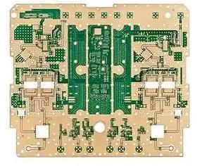
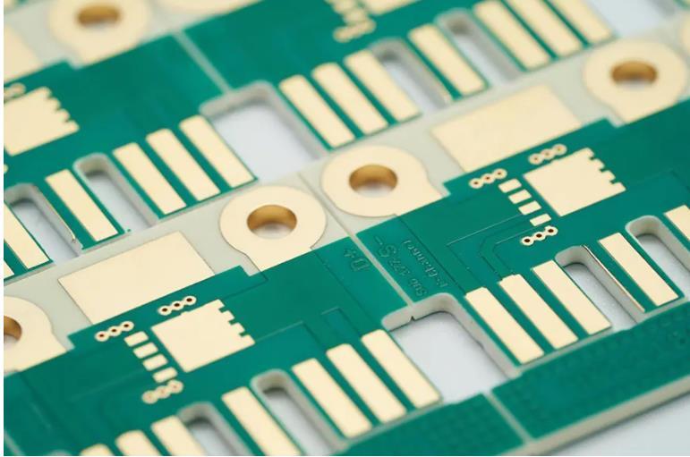
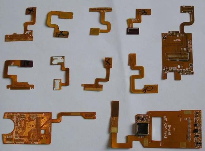

China Chaosheng Electronic Intelligent Products Multilayer Circuit Board HDIPCB TechnologyPCB
Automotive electronics PCB, Medical equipment circuit board, Industrial control PCB, Aerospace & military grade PCB, Ion‑equipment high‑voltage board, High‑speed server PCB, 5G communication circuit board, Radar RF microwave PCB, Wireless terminal motherboard, Industrial SBC mainboard, High‑power industrial control PCB, Automation controller board, Drone flight‑control PCB, Robot control board, High frequency low loss PCB, Thick hard gold finger circuit board, HDI blind & buried via PCB
China Chaosheng Electronic Medical Equipment Products Multilayer Circuit Board HDIPCB Technology
Automotive electronics PCB, Medical equipment circuit board, Industrial control PCB, Aerospace & military grade PCB, Ion‑equipment high‑voltage board, High‑speed server PCB, 5G communication circuit board, Radar RF microwave PCB, Wireless terminal motherboard, Industrial SBC mainboard, High‑power industrial control PCB, Automation controller board, Drone flight‑control PCB, Robot control board, High frequency low loss PCB, Thick hard gold finger circuit board, HDI blind & buried via PCB
China Chaosheng Electronic Automotive Products Multi layer Circuit Board HDIPCB Technology
Ultra thin PCB,Double layer ultra-thin PCB,Multi layer ultra-thin PCB,HDI ultra-thin PCB,Oversized thin board PCB,Flexible Rigid PCB,PCB factory,Top PCB Manufacturers,Printed Circuit Board (PCB),If you get rid of the PCB,PCB Piezotronics,PCB Simulation,Certified PCB Design Company,Quick Turn PCB
China Chaosheng Automotive Control Multi layer Circuit Board PCB Source Factory
Ultra thin PCB,Double layer ultra-thin PCB,Multi layer ultra-thin PCB,HDI ultra-thin PCB,Oversized thin board PCB,Flexible Rigid PCB,PCB factory,Top PCB Manufacturers,Printed Circuit Board (PCB),If you get rid of the PCB,PCB Piezotronics,PCB Simulation,Certified PCB Design Company,Quick Turn PCB
Surrounding dam metal ceramic circuit board PCB
- ✅ High airtightness: Metal dam sealed cavity, protecting chips and extending their lifespan (essential for military/aerospace industries). - ✅ Super heat dissipation: Ceramic thermal conductivity is 100 times that of FR-4, suitable for high-power LED, laser, IGBT modules. - ✅ High reliability and stability: Low thermal expansion coefficient (CTE ≈ 4-7 ppm/℃), matched with silicon chips, resistant to thermal shock and high and low temperatures. ✅ ** Large scale mass production: Chaosheng has a unique 3m × 1.24m production line that can produce ≥ 500 pieces per month, replacing multi board splicing and improving system stability.
18layer coil inductor multilayer board PCB
Product Name: Aerospace, Military, Nuclear, Unmanned Aerial Vehicle ProductsBoard: FR-4, TG150Layers: 18layer coil inductor multilayer board PCBMinimum line width/spacing: 8/8milFinished product size: 255x176mm/1 * 1pcsSurface technology: Sinking gold, green oilCopper thickness: Inner and outer layers of copper with a thickness of 175umPlate thickness: 3.50mmMinimum aperture: 0.35mm, laser hole/mm,Transport Package:Vacuum packaging+moisture-proof beads+separated white paper+cardboard box+wooden card boardFeatures: Difficulties such as dense inner and outer coilsUsage: Engine, electric motor, inductor, orange equipment, etc2-80 layers of rigid circuit boards, 2-50 layers of flexible circuit boards and PCBA productionChaosheng Group Company mainly produces product categoriesHigh end double-sided, multi-layer, flexible, high-frequency, HDI interconnect, metal based, high thermal conductivitymetal based, ceramic, cut in metal based, cut in buried capacitor, cut in thick copper buried magnet, concave convex step substrate, 5G high-speed board, thick copper, thick gold, high carbon resistance, double-sided multi-layerMiNiLED, MiNiHDILED, MiNiOLED, IC carrier substrate, roll to roll FPC, long FPC, large-sized printed circuit board,halogen-free material, high-frequency material, high-speed material, metal material, environmentally friendly circuit board, blind buried hole circuit board, high thermal conductivity aluminum based, thermoelectric separation copper based, PDU busbar, iron-based and metal based (core) mixed pressure plate, embedded copper buried copper. Buried resistance buried capacitance buried ceramic bead board, ultra-thin BT board, ceramic substrate, IC carrier board,high-frequency mixed voltage, high-speed board, differential impedance board, thick copper plate, thick gold platedboard, HDI An integrated OEM and ODM production factory for Anylayer, double-sided, multi-layer, HDI FPC, softhard combination HDI, roll to roll FPC, ultra long FPC, ultra large size PCB production and product design and development, software development, special material printed circuit boards, etc. Process Capability TableTechnical ltemMassProductAdvanced Technology2015 2021 2025 Max.Layer Count80 layer100 layer100 layerPCB through hole board2~80 layer2~100 layer2~100 layerMaximum size through hole 1~237〞*98.50"43.3〞*118.11"43.3〞*118.11"Minimum line width and spacing10(0.40)10(0.40)7.50(0.30mm)Minimum mechanicalhole(mm)12(0.50)10(0.40)8.50(0.35mm)Maximum size through hole 4~22layers37〞*43.30"43.3〞*43.30"43.3〞*43.30"Maximum size through hole 4~22layers31.50 ″*59"31.50 ″*70.86"31.50 ″*70.86"Maximum size through hole 4~22layers10(0.40)10(0.40)7.50(0.30mm)Minimum line width and spacing formulti-layer large-sized PCBs10(0.40)10(0.40)7.50(0.30mm)Maximum size of multi-layer through-hole : 4-22 layers with the smallesthole12(0.50)10(0.40)8.50(0.35mm)Maximum size HDI 4~36 layers31.50 ″*55"31.50 ″*55"31.50 ″*55"Minimum line width and linespacing of large size PCBThrough hole 12 /12milHDI14 /14milThrough hole 10/10milHDI12 / 12milThrough hole 8 /8milHDI12 / 12milThe largest board ruler 1 → thesmallest hole of 18 layersThrough hole0.50mmHDI :0.45mmThrough hole 0.50mmHDI : 0.45mmThrough hole0.50mmHDI : 0.45mmThe layer number of FPC1~36layer1~60layer1~60layerMaximum size offlexible FPC19.68〞*55"28〞*59"31.49〞*118.12"Maximumsize of flexible FPC with soft hardcombination19.68〞*55"28〞*59"31.49〞*118.12"FPC (roll to roll) maximum size19.68 ″*7874"19.68 ″*7874"19.68 ″*7874"Maximum size of FPC single chipshipment19.68 ″*118.11"19.68 ″*196.8"19.68 ″*196.80"The layer number of FPC2~18 layer2~36 layer2~42 layerMaximum size of layered board19.68 ″*35"19.68 ″*43"19.68 ″*43"Number of through-hole layers2~20layer2~30 layer2~40 layerHard and soft HDI layers2~14 layer2~18 layer2~22 layerMaximum size of soft and hardcombination19.68 ″*43"19.68 ″*49"19.68 ″*49"FPC/soft-hard combinationarbitrary interconnection HDI4+X+4InterconnectHDI5+X+5Interconnect HDI6+X+6InterconnectHDIHDIPCB layers4~36layer4~60layer4~80 layerAnylayer HDI PCB4+X+4InterconnectHDI5+X+5、Interconnect HDI8+X+8、InterconnectHDIHDIPCB maximum board size24"*52"43"*49"43"*49"Number of through hole layers ofhigh frequency board2~18 layer2~36 layer2~60 layerHDI layersofhighfrequency board2~16 layer2~24 layer2~60layerMaximum size ofhigh frequency board37 ″*43"43 ″*49"43 ″*49"Number of ceramic plates1-2 layer1~4 layer1~6 layerCeramic plate thickness0.60mm-1.60mm0.38mm-20.0mm0.38mm-20.0mmMaximum size of ceramic plate100*150mm150*190mm150*650mmMinimum aperture of ceramicplate0.50mm0.35mm0.35mmMinimum line width and linespacing of ceramic board16/16mil12/12mil10/10milNumber of layers of metalcopper substrate1-2 layer1~4 layer1~6 layerMaximum line width and linespacing of metal iron substrate12/12mil4/4mil4/4milNumber of layers of metalaluminum substrateHDI1-2 layer1~4 layer1~6 layerMaximum size of metal substrate37 ″*43"25.59 ″*59"25.59 ″*59"The smallest hole ofthe metal substrate0.50mm0.35mm0
64 layer thick copper coil plate technology
Product Name: Aerospace, Military, Nuclear, Unmanned Aerial Vehicle ProductsBoard: FR-4, TG150Layers: 64 layer coil inductor multilayer board PCBMinimum line width/spacing: 8/8milFinished product size: 301x301mm/1 * 1pcsSurface technology: Sinking gold, green oilCopper thickness: 105um for inner and outer layersPlate thickness: 5.5mmMinimum aperture: 3.5mm, laser hole/mm,Features: Difficulties such as dense inner and outer coilsUsage: Engine, electric motor, inductor, orange equipment, etcFirstly, from the perspective of the company's own technological strength, Chaosheng clearly has the ability to produce high multi-layer circuit boards, with its product range covering 2-80 layers of precision multi-layer circuit boards.At the same time, Chaosheng also has imported fully automated precision equipment production lines and a sound quality management system. It has passed multiple quality system certifications such as UL and ISO9001 in the United States, which has laid the foundation for its production of 64 layer and other ultra-high multi-layer circuit boards. Secondly, from the perspective of product characteristics, the product adopts a design that combines blind grooves and depth control grooves, combined with metal edging. The middle part has been treated with immersion gold, which not only improves corrosion resistance but also enhances stability.It is speculated that a 64 layer inductor coil metal wrapped circuit board may also use a similar design to meet the needs of multi-layer and different thickness circuit fabrication.At the same time, metal edging can effectively shield electromagnetic radiation, further enhancing signal integrity and circuit stability. Finally, for the part of the inductor coil, precise control of the inductance value may be achieved through special layout design of the coil and optimized via settings, in order to meet specific electrical performance requirements of the product. A multi-layer coil PCB (Printed Circuit Board) refers to a type of circuit board that consists of multiple layers of conductive material, separated by insulating layers, and is often used for applications requiring compact designs, such as RF (radio frequency) coils, inductors, transformers, and other electromagnetic components.### Key Features of Multi-Layer Coil PCBs:1. **Layer Structure**: - Multi-layer PCBs typically consist of three or more layers. The inner layers can be used for routing power and ground, while the outer layers can be utilized for signal routing and component placement.2. **Coil Design**: - The coils can be designed in various configurations, such as solenoids, toroids, or planar coils, depending on the application. The design may include various winding techniques and geometries to optimize inductance and performance.3. **Material**: - Common materials used for multi-layer PCBs include FR-4 (a type of fiberglass epoxy), Rogers materials (for high-frequency applications), and other specialized materials that can handle specific thermal or electrical requirements.4. **Impedance Control**: - For RF applications, controlling the impedance of the coil is crucial. Multi-layer designs can help maintain consistent impedance across the PCB by using specific layer stack-ups and trace widths.5. **Thermal Management**: - Multi-layer PCBs can help dissipate heat more effectively than single-layer designs. Proper thermal management is essential in coil applications, especially when dealing with high currents.6. **Manufacturing Process**: - The fabrication of multi-layer PCBs involves several steps, including layer alignment, lamination, drilling, plating, and etching. Advanced techniques such as laser drilling and via filling may be employed to create vias and interconnections.7. **Applications**: - Multi-layer coil PCBs are used in various applications, including: - RF and microwave devices - Wireless charging systems - Inductive sensors - Power amplifiers - Communication devices### Design Considerations:1. **Simulation**: - Using simulation software (like HFSS, CST, or other electromagnetic simulation tools) to model the coil's behavior can help in optimizing its design before fabrication.2. **Manufacturing Tolerances**: - Ensure that the PCB manufacturer can meet the necessary tolerances for the coil's dimensions and layer alignment to achieve the desired performance.3. **Testing and Prototyping**: - Prototyping the design and conducting tests (like S-parameter testing) is essential to validate performance and make any necessary adjustments.4. **Cost**: - Multi-layer PCBs can be more expensive than single-layer boards due to the complexity of manufacturing and the materials used. Balancing performance requirements with cost considerations is crucial.5. **Stack-Up Design**: - Carefully planning the stack-up of the PCB layers is important to achieve the desired electrical performance and to minimize issues like crosstalk and electromagnetic interfe
ultra-thin ceramic circuit boards (PCBs) are like a shining star
Ceramic circuit board PCB Aluminum oxide ceramic PCB Aluminum nitride ceramic PCB 96.6% alumina ceramic PCB Aluminum nitride 96.6% ceramic PCB 99.9% alumina ceramic PCB Aluminum nitride 96.6% ceramic PCB Multilayer ceramic circuit board PCB
Phone: 13528819118
Email: sales@chaoshengpcb-fpc.com
Office address: 101, No.2 Longhe Road,
Longgang District, Shenzhen,
Guangdong, China
(Cha Bajie Headquarters) 2nd Floor
Chaosheng Electronics)
Hong Kong Address: Chungking Mansion,
36-44 Nathan Road, Tsim Sha Tsui, Kowloon,
Hong Kong, China

Sales Department2:616674225
Sales Department销售部:373011007
Tel:+86-13528819118
Email:sales@chaoshengpcb-fpc.com
WhatsApp:13528819118
Skype:pcb-fpcb88@163.com