

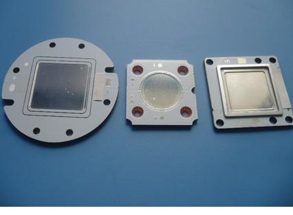
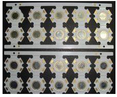


2L mirror aluminum based PCB
2L mirror aluminum based PCB Product field: New energy vehicles Layers: 2L Plate thickness: 2.0mm Process structure: Mirror aluminum+2L aluminum base+deep head hole Surface treatment: silver deposition
key word:
Products and services
and
product
of
the
2L mirror aluminum based PCB
Product Description
Product field: New energy vehicles
Layers: 2L
Plate thickness: 2.0mm
Process structure: Mirror aluminum+2L aluminum base+deep head hole
Surface treatment: silver deposition
| Main Product Structure of Chaosheng Group Company 2-80 layers of rigid circuit boards, 2-50 layers of flexible circuit boards and PCBA production Chaosheng Group Company mainly produces product categories High end double-sided, multi-layer, flexible, high-frequency, HDI interconnect, metal based, high thermal conductivity metal based, ceramic, cut in metal based, cut in buried capacitor, cut in thick copper buried magnet, concave convex step substrate, 5G high-speed board, thick copper, thick gold, high carbon resistance, double-sided multi-layer MiNiLED, MiNiHDILED, MiNiOLED, IC carrier substrate, roll to roll FPC, long FPC, large-sized printed circuit board, halogen-free material, high-frequency material, high-speed material, metal material, environmentally friendly circuit board, blind buried hole circuit board, high thermal conductivity aluminum based, thermoelectric separation copper based, PDU busbar, iron-based and metal based (core) mixed pressure plate, embedded copper buried copper. Buried resistance buried capacitance buried ceramic bead board, ultra-thin BT board, ceramic substrate, IC carrier board, high-frequency mixed voltage, high-speed board, differential impedance board, thick copper plate, thick gold plated board, HDI An integrated OEM and ODM production factory for Anylayer, double-sided, multi-layer, HDI FPC, soft hard combination HDI, roll to roll FPC, ultra long FPC, ultra large size PCB production and product design and development, software development, special material printed circuit boards, etc. The main application areas of PCB and PCBA products of Chaosheng Group Company Communication terminals, communication stations, electronic communication, fiber optics, optical modules, backlight sources, chip systems, communication equipment, communication instruments, computers, intelligent devices, intelligent control, system control, industrial power control, industrial equipment, testing instruments, testing instruments, SD cards, SG cards, mobile phones, computers, various antennas, radars, automobiles, light sources, resistors, music equipment, playback equipment, banking equipment, medical instruments, medical equipment, aerospace, aviation, military, LED, OLED, OLCD power control power supply, industrial power supply, communication power supply, automotive power supply, office equipment, digital products, computers and other application fields; The main application areas of flexible circuit boards (FPC) and FPCA products of Chaosheng Group Company Hard drives, printers, fax machines, scanners, sensors, mobile phones, connectors, modules, walkie talkie antenna cards, high-end cameras, digital cameras, laser heads, CDs, medical devices, instruments, drives, automobiles, automotive instruments, automotive drive disks, drivers, optical drives, medical devices, medical equipment, backlight sources, modules, banking equipment, industrial instruments, LED light strips, military, aviation, aerospace, national defense and other product fields.  |
|||||||||||||||
| Serial Number | Project | Manufacturing capability | |||||||||||||
| 1 | Layers | Floors 1-80 | |||||||||||||
| 2 | Maximum size of PCB | 2500*1150mm | |||||||||||||
| 3 | Maximum size of flexible FPC | 500mm*100m | |||||||||||||
| 4 | Maximum size of PCBA | 1600mm*1000mm | |||||||||||||
| 5 | FPCBA maximum size | 500mm*100m | |||||||||||||
| 6 | PCB finished product thickness | 0.15-12.0mm | |||||||||||||
| 7 | Thickness of flexible FPC finished product | 0.05-0.60mm | |||||||||||||
| 8 | Finished copper thickness | 12um-1075um | |||||||||||||
| 9 | Minimum finished aperture of laser hole | 0.075mm | |||||||||||||
| 10 | Minimum line width and spacing | 1.5mi/1.50mil | |||||||||||||
| 11 | Minimum finished hole diameter for through-hole | 0.15mm | |||||||||||||
| 12 | Thickness stacking aspect ratio | 1:35 | |||||||||||||
| 13 | By processing methods | VIA blind buried hole treatment: ink plug hole, resin plug hole, copper paste plug hole, VCP copper filling hole, silver paste plug hole, carbon oil plug hole, etc | |||||||||||||
| 14 | Surface Treatment | Sinking gold, electroplating nickel gold, electroplating thick gold, electroplating gold+OSP, electroplating nickel gold+sinking gold, electroplating nickel gold+sinking gold+OSP, electroplating gold+OSP, electroplating gold+gold fingers, OSP+gold fingers, lead-free tin spraying, lead-free tin spraying+sinking gold, lead-free tin spraying+gold fingers, lead tin spraying, OSP, sinking tin, sinking silver, electroplating silver | |||||||||||||
| 15 | Main substrate brands | Rogers, Arlon, Taconic, TP-2, Megtron, Neclo, Isola, F4B, 3M, Mitsui Group (Japan Mitsui/Mitsui Top), Taiyo TUC, Taiguang EMC, Tenghui VT, Shengyi SY, Lianmao ITEQ, South Asia NOUYA, DuPont Kappon, Taihong, Hongren Hongren, Xin Yang, Nippon Steel Nippon Stee, Teflon, Yasen, Matsushita, RCC, Mitsui Mitsui Group (Japan Mitsui Top), 3M (USA) 3M Location, Kyocera CERADIR, Jiuhe, Jiuhao, China Porcelain, Huaqing, Ai Shengda, Slitton, Kai Changde, Tongxin, Bergs, Yalong, Taiconieta, etc | |||||||||||||
| 16 | Solder mask color | Green, black, red, yellow, white, blue, purple, matte green, matte black, etc | |||||||||||||
| 17 | Test service | AOI、X-Ray、 Voltage withstand test, short circuit test, soldering test, thermal shock test, functional test, high temperature and high humidity test, first piece tester, etc | |||||||||||||
| 18 | Molding method | CNC shape, punch shape, V-CUT+forming method | |||||||||||||
| 19 | Finished product warpage | ≤0.5% | |||||||||||||
| 20 | Mechanical aperture tolerance | ≤0.025mm | |||||||||||||
| 21 | Finished product warpage | ≤0.5% | |||||||||||||
| 22 | MiNiLED Minimum PAD | 0.065mm/0.065mm | |||||||||||||
| 23 | Thermal conductivity | ≧8W | |||||||||||||
| 24 | Highest withstand voltage | 2500Pa | |||||||||||||
| 25 | High carbon resistance value and tolerance | ≧100→15000Ω±20% | |||||||||||||
| 26 | Impedance tolerance | ≤5→8%Ω | |||||||||||||
| 27 | IC Carrier Board Series | Minimum line width and spacing of 20um/20um | |||||||||||||
| FAQ | |||||||||||||||
| Question Point | Answer | ||||||||||||||
| Q: What information is required for PCB | CEGSATE: Gberber files for PCB production, product process instructions, such as material requirements, surface treatment requirements, finished product thickness requirements, PCB stack structure diagram for advanced products, copper thickness requirements for each layer, sample quantity requirements, batch order requirements, product application fields, and other related information are required | ||||||||||||||
| Q: What information does PCBA need to provide | CEGSATE: BOM report is required (including the brand, specifications, and model of the components), X and Y coordinate numbers of PCBA components, and processing requirements: Do we need to purchase the components on our behalf? Or customer supplied components? Do you need software burning? What is the required quantity? What is the monthly demand and other detailed information. | ||||||||||||||
| Question: Is my file secure? | CEGSATE: Your files are very secure, and we protect intellectual property rights for our clients throughout the entire process. All files provided by the customer will never be shared with any third party. | ||||||||||||||
| Q: What is the minimum order quantity? | CESGATE: There is no minimum order quantity in POE. We are able to handle small and large batches flexibly. | ||||||||||||||
| Q: Do you have any other services? | CESGATE: We mainly focus on PCB+FPC production+SMT+assembly PCBA+component procurement services; In addition, we can also provide programming, testing, software burning, wiring, and shell assembly services; And product design, product development, software development | ||||||||||||||
| Q: What is your inspection method? How do you control the quality? | CESGATE: In order to ensure the quality of PCB and FPC products, flying pin testing is usually used for samples and small batches; The inner circuit undergoes AOI optical inspection, online AOI inspection, and the finished product undergoes 100% inspection through E-SET testing rack. The appearance undergoes 100% inspection through fully automatic finished product inspection equipment and FQC. PCBA undergoes automatic optical inspection (AOI), BGA part X-Ray 100% radiographic inspection, and first article inspection (FAI). PCBA products that require software burning undergo 100% full testing through finished product testing rack according to product functional requirements. | ||||||||||||||
A 2-layer mirror aluminum-based PCB (Printed Circuit Board) is a specialized type of PCB that combines the excellent thermal conductivity of aluminum with a reflective, smooth surface finish, offering superior performance in high-power and heat-sensitive electronic applications. Unlike conventional FR4 boards, aluminum PCBs feature a metal substrate—typically aluminum or an aluminum alloy—bonded with an insulating layer and a copper circuit layer. The mirror finish not only enhances aesthetic appeal but also improves light reflection in LED applications, making them ideal for high-efficiency lighting solutions.
Structure and Design
The typical 2-layer aluminum-based PCB consists of three main layers: a copper circuit layer, a dielectric insulation layer, and an aluminum base layer. The copper layer carries the electrical signals, while the dielectric layer ensures insulation and facilitates heat transfer from the components to the aluminum base. The mirror aluminum surface provides a highly reflective platform, which is especially useful for applications where light management and thermal dissipation are critical.
Compared to standard single-layer aluminum PCBs, the 2-layer configuration allows for more complex circuit designs and enables higher-density component placement. Designers can optimize trace routing and component arrangement without compromising thermal management, making 2L mirror aluminum PCBs suitable for compact and high-performance electronic devices.
Material Advantages
Aluminum substrate offers high thermal conductivity, mechanical strength, and excellent electrical insulation through the dielectric layer. The mirror finish further enhances thermal radiation, allowing components to operate at lower temperatures, extending lifespan, and improving reliability. Additionally, aluminum PCBs are lightweight yet robust, providing a durable solution for industrial, automotive, and consumer electronics.
The 2-layer design allows separation of signal and power lines, reducing electromagnetic interference (EMI) and improving signal integrity. This is particularly valuable in sensitive devices like medical instruments, communication equipment, and precision measurement systems.
Applications
2L mirror aluminum-based PCBs are widely used in LED lighting, power electronics, automotive electronics, and telecommunication equipment. In LED modules, the reflective mirror surface enhances light efficiency by redirecting light emitted from diodes, reducing energy consumption while increasing illumination output. In power electronics, aluminum PCBs provide efficient heat dissipation for components like power transistors, MOSFETs, and voltage regulators.
In automotive electronics, these PCBs are employed in headlights, tail lights, control modules, and electric vehicle battery management systems. Their superior thermal management ensures reliability in high-temperature environments and supports compact design, crucial for modern vehicles.
Manufacturing Process
The production of 2L mirror aluminum-based PCBs involves several critical steps: substrate preparation, copper lamination, circuit patterning, etching, dielectric layer bonding, surface finishing, and testing. High precision is required in each stage to maintain surface smoothness and reflectivity. Advanced technologies such as CNC milling, laser ablation, and surface polishing ensure mirror-like finishes and precise circuit geometries.
Quality control is essential to prevent defects such as warping, delamination, or uneven reflection, which could compromise thermal performance and electrical reliability. Manufacturers often use automated optical inspection (AOI) and thermal imaging to verify integrity before shipment.
Market Trends
The demand for aluminum PCBs, especially 2L mirror types, has been rising due to rapid growth in LED lighting, 5G communication infrastructure, and electric vehicles. The high efficiency, durability, and thermal management capabilities of these PCBs make them a preferred choice for high-power applications. Global suppliers are investing in research and development to enhance substrate materials, dielectric performance, and mirror surface techniques to meet evolving industry standards.
Advantages over Conventional PCBs
Compared to traditional FR4 or standard copper PCBs, 2L mirror aluminum-based PCBs offer:
-
Superior heat dissipation for high-power components.
-
Enhanced light reflection for LED applications.
-
Greater mechanical strength and durability.
-
Reduced electromagnetic interference and improved signal integrity.
-
Lightweight yet robust construction, suitable for compact designs.
Conclusion
2L mirror aluminum-based PCBs represent a critical advancement in high-performance electronics. Their combination of thermal efficiency, structural durability, and reflective surface properties makes them essential in applications ranging from LED lighting to automotive and telecommunication electronics. As industries continue to demand higher performance, efficiency, and miniaturization, 2L mirror aluminum PCBs will play an increasingly vital role in next-generation electronic devices.
Related products

China Chao Sheng Electronic Automotive-Grade Hard-Soft Combined HDI-FPC
China Chaosheng Electronic Intelligent Products Multilayer Circuit Board HDIPCB TechnologyPCB
China Chaosheng Electronic and Electrical Products Multi layer Circuit Board PCB Source FactoryPCB
China Chaosheng Electronic Medical Equipment Products Multilayer Circuit Board HDIPCB Technology
China Chaosheng Electronic Automotive Products Multi layer Circuit Board HDIPCB Technology
China Chaosheng Automotive Control Multi layer Circuit Board PCB Source Factory
China Chaosheng Electronics Mobile Phone Flexible Motherboard FPC
China Chaosheng Electronic Printer Driver Flexible FPC
blind buried hole HDI flexible FPC,4-layer flexible FPC
Surrounding dam metal ceramic circuit board PCB
18layer coil inductor multilayer board PCB
64 layer thick copper coil plate technology
The following is a detailed introduction about "PET carbon wire pseudo double-layer flexible FPC"
Transparent PCB, transparent flexible FPC
Detailed Introduction to Transparent FR-4 Multilayer PCB
Welcome to inquire
Phone: 13528819118
Email: sales@chaoshengpcb-fpc.com
Office address: 101, No.2 Longhe Road,
Longgang District, Shenzhen,
Guangdong, China
(Cha Bajie Headquarters) 2nd Floor
Chaosheng Electronics)
Hong Kong Address: Chungking Mansion,
36-44 Nathan Road, Tsim Sha Tsui, Kowloon,
Hong Kong, China

Sales Department2:616674225
Sales Department销售部:373011007
Tel:+86-13528819118
Email:sales@chaoshengpcb-fpc.com
WhatsApp:13528819118
Skype:pcb-fpcb88@163.com